• For details about Moxtek employment opportunities, please visit the Careers page

  • This field is for validation purposes and should be left unchanged.
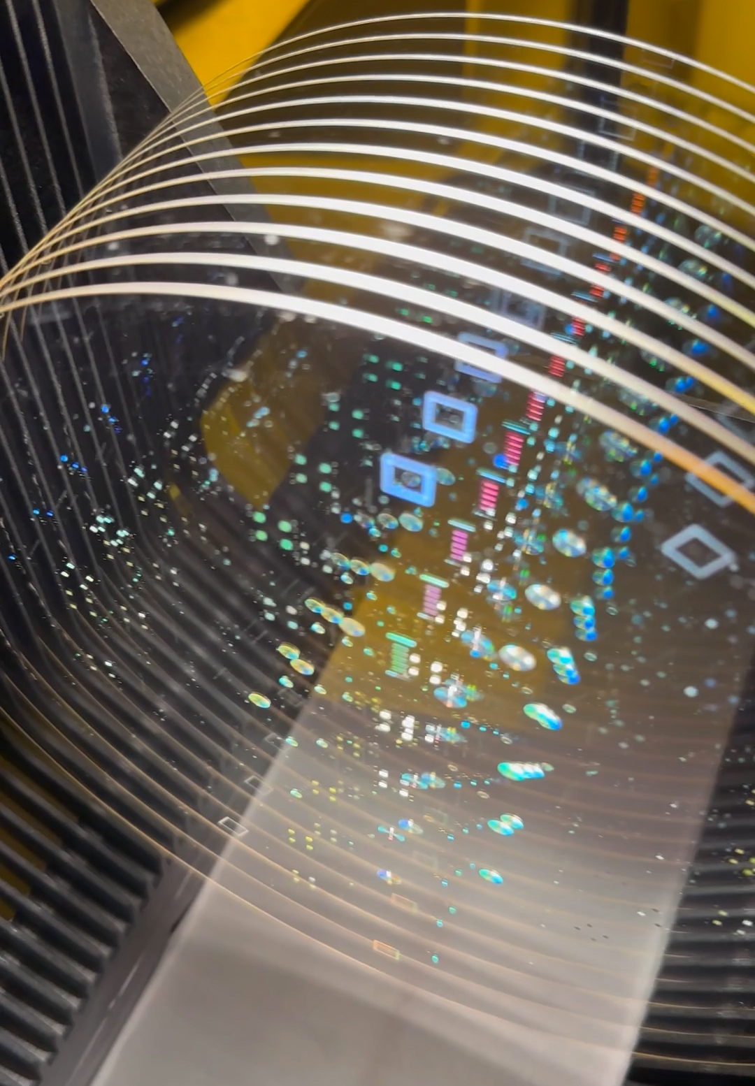
Metalens on 8'' Wafers
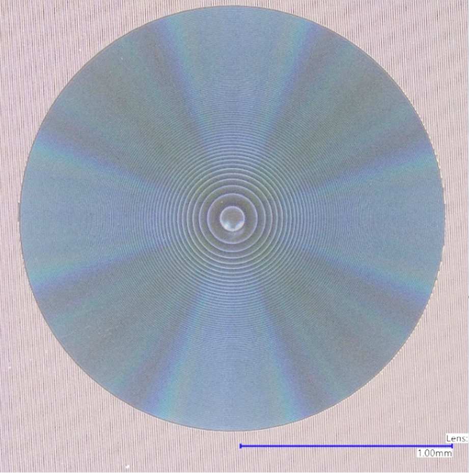
2mm Metalens
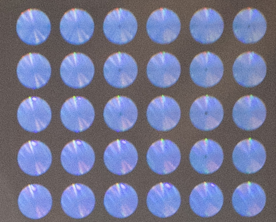
Metalens Array
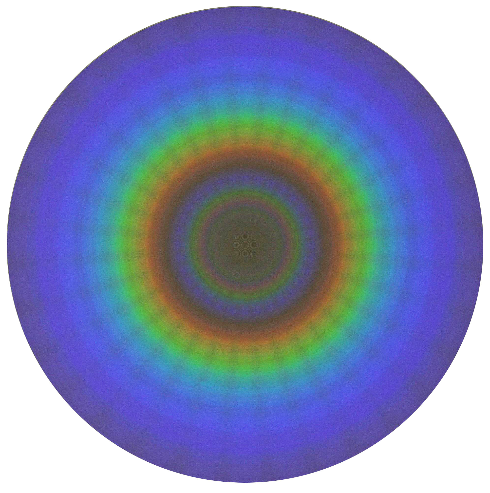
5mm Metalens

Metalens on 8'' Wafers
Polarizer Comparison Tool

2mm Metalens
Polarizer Comparison Tool

Metalens Array
Polarizer Comparison Tool

5mm Metalens
Polarizer Comparison Tool

Metalens Foundry

Moxtek has been manufacturing nanoscale structures for over 20 years. We have developed efficient methods to create e-beam masters combined with our existing NIL processing to provide a full solution approach to volume production. Moxtek can optimize the lens design to match customers applications. Moxtek offers design, fabrication, measurement, and packaging capabilities. Moxtek has production facilities in USA, Japan, and China.

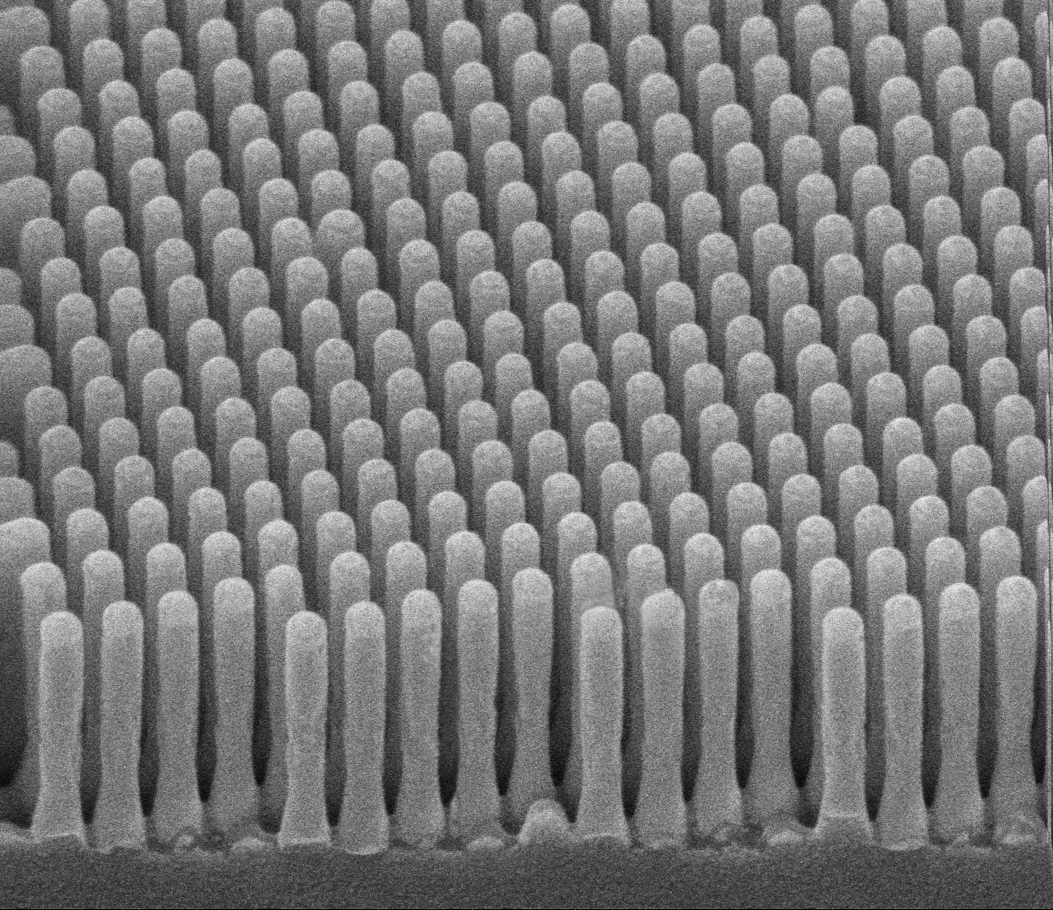
Manufacturing Metalenses for the visible range imparts demanding nanofabrication requirements. To manufacture metalenses and other metastructured devices in volume, Nanoimprint Lithography (NIL) becomes a key enabling technology. Moxtek has used NIL to successfully demonstrate scalability and the ability to reliably replicate metalenses with extremely tight tolerances, including variations in local spacing. By using the NIL relief structure to etch high refractive index, high aspect ratio niobium oxide nanostructures, Moxtek has produced a variety of visible metalenses with different focal lengths. Building on years of expertise, Moxtek has developed reliable methods to manufacture wafer-scale visible metalenses for various emerging applications.        

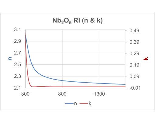
Niobium Oxide Index of Refraction and Extinction Coefficient

Moxtek Advantages
  • Uniform lens replication over Ø200mm wafer
  • Production and prototype compatible processes
  • Niobium oxide (Nb2O5) has proven beneficial in ease of deposition, uniform etching, and lower cost
  • Ability to replicate customer designs
  • Experience with thin-film deposition, etching, and NIL
  • In-house metalens modeling
  • Flexibility in lens parameters
  • Protective overcoat enhances durability and performance
Design Parameters
  • Minimum CD: 50nm
  • Minimum Space Gap: 70nm
  • Thickness: ≤1,000nm
  • Aspect Ratio: 12:1
  • Meta Materials (preferred): Nb2O5, Al
  • Meta Materials (other): Si, SiO2, Si3N4
  • Substrate Diameter: Ø200mm diameter
  • Substrate Thicknesses: 0.7mm to 1.6mm thick
  • Substrate Types: Display glass, Fused Silica, Silicon, Sapphire